Equipment
The tools below can be reserved using the:
Thin Films/Etch Area
-
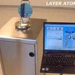
Atomic Layer Deposition System
Conformal coating of oxides.
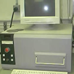
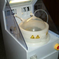
The principle of ALD is based on sequential pulsing of chemical precursor vapors, both of which form about one atomic layer each pulse. This generates pinhole free coatings that are extremely uniform in thickness, even deep inside pores, trenches and cavities. The system accepts a single 4" wafer and the user selects the recipe and the number of cycles to determine the thickness desired. Available precursors include: Aluminum, Zirconium, Hafnium, Gallium and Titanium. Other precursors purchased by the user may be installed by Staff. Precursors must be purchased (In cartridges "For use in ALD systems")
-
Tool #11 CVD Furnace
The Low Pressure Chemical Vapor Deposition system (LPCVD, tool #11) is a 4- stack furnace manufactured by CVD Equipment Corp. The furnace tubes feature critically controlled temperatures and gas flows to achieve the correct environment to grow layers of oxide and to deposit chemical layers onto the silicon substrates. These layers form the basis of the structures that are produced in the subsequent lithography and etching processes.
- Tube # 1 is equipped for Wet Oxidation using a Liquid source at temperatures up to 1200 C
- Tube # 2 is equipped for Dry Oxidation at temperatures up to 1200 C
- Tube # 3 is equipped for Low Pressure Chemical Vapor Deposition of Silicon Nitride at temperatures up to 900 C
- Tube # 4 is equipped for Low Pressure Chemical Vapor Deposition of Polysilicon at temperatures up to 800 C
There is currently no Procedure Manual available for download for this tool.
-
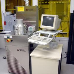
Tool #3 PECVD System
The Plasma Enhanced Chemical Vapor Deposition system (PECVD, tool #3) is a Plasmatherm 790 engineered for research, development, and pilot production using Plasma Enhanced Chemical Vapor Deposition. This process is performed in a reactor at temperatures up to 400 deg. C. The deposited film is a product of chemical reactions of the source gases supplied to the reactor. A plasma is generated in the reactor to increase the energy available for the chemical reaction to take place.
-
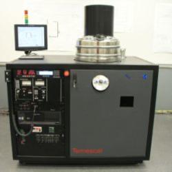
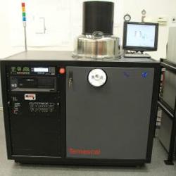
Tool #4 E-Beam Evaporator 1Tool #4A E-Beam Evaporator 2
The E-Beam Evaporators (tool #4 and 4A) are Temescal BJD 1800 systems designed for Universities and Research and Development operations. The systems focus a beam of electrons onto a metal target in a crucible to apply a thin metal film onto substrates by evaporation in a high vacuum. The thickness is controlled by electronic feedback systems, and specific tooling geometries allow excellent coverage to be achieved on a variety of substrate sizes up to a diameter of 4''. A total of 7 four inch wafers can be processed per run. Tool #4 (Evaporator #1) Can be operated in manual deposition mode and a variety of materials are allowed to be evaporated. Tool #4A (Evaporator #2) Must be operated in Auto deposition mode only with Gold, Chrome, Titanium, Palladium, Aluminum or Nickel. The user just selects the material and final thickness and the tool does the rest.
-
Tool #5 Thermal Evaporator
The Thermal Evaporator (tool #5) is also a Temescal BJD 1800 system similar to the E-beam evaporator. (tool #4) This system applies thin-films of various metals onto substrates by evaporating metal in a high vacuum, however the Thermal Evaporator heats the material by passing electrical current through a filament much like a light bulb. The filament is designed with a dimple in the middle to accommodate the material to be evaporated. The thickness is controlled by electronic feedback systems, and specific tooling geometries allow excellent coverage to be achieved on a variety of substrate sizes up to a diameter of 4''.
There is currently no Procedure Manual available for download for this tool.
-
Tool #52 Rapid Thermal Annealer (RTA)
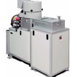
The Rapid Thermal Anneal system (tool #52) is manufactured by Modular Process Technology Corp. The RTP-600S is a rapid thermal processing system, which uses high-intensity visible radiation to heat a single wafer for a short time at precisely controlled temperatures. These control capabilities, combined with the heating chamber's cold-wall design and thermal uniformity, provide significant advantages over conventional furnace processing. Temperatures up to 800 deg. C with a thermocouple and 1,300 deg. C with a pyrometer can be reached in seconds. Applications include: Ion Implant activation, Polysilicon annealing, Oxide reflow, Silicide formation, Contact alloying, Oxidation and Nitridation and Compound semiconductor processing.
-
Tool #53 Reactive Ion Etch System (RIE)
STS Reactive Ion Etcher (RIE) dielectric System is designed for isotropic RIE plasma etching of dielectric films. The system is capable deep etching of oxide with high selectivity to resist and silicon and fast etch rates. The RIE plasma etching process is accomplished through the use of a low pressure; 13.56 megahertz radio frequency (RF) induced gaseous discharge. The system is set to handle four different gases (CF4, CHF3, O2, and He) for etching of Silicon Nitride or Silicon Dioxide at various etch rates. The sample is backside cooled during etch processes.
-
Tool #8A Spin Rinser Dryer
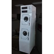
The Semitool model 870 Spin Rinser Dryer handles cassettes of 4" wafers. The system rinses with de-ionized water then spins and dries with nitrogen.
There is currently no Procedure Manual available for download for this tool.
-
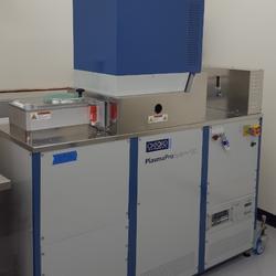
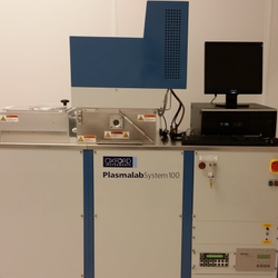
Tool #54 ICP Etch System
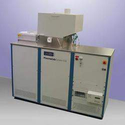
The Inductively Coupled Plasma Universal etching system (tool #54) is an Oxford Plasmalab 100/180 model with vacuum load-lock that accommodates up to 6'' diameter wafers. Chlorine-based gases are used for etching semiconductors and some metals and Flourine-based gases provide deep Trench Etching capability in Silicon. Typical semiconductor materials that are etched are: AlGaAs, InGaAs, AlGaSb, GaN, and Si. Metals that can be etched include Al, Ti, and thin Pt layers. The 300 watt RF system produces a high-density, low- pressure, low-energy inductively coupled plasma. This type of plasma allows high selectivity and aspect ratio etching for depths greater than 250 microns. The system control is via a standard PC, which automatically loads a wafer into the process chamber. Once in the chamber, the wafer is placed onto a helium-cooled chuck during the process. The substrate is RF-biased independently of the inductively coupled RF plasma, which results in low ion energies and thus low ion bombardment. Consequently, an ICP system will provide high chemical etch selectivities with high etch rates. Process gases available are: N2, BCl3, Cl, C4F8, Sf6, CF4, He, O2, Ar, SiCl4 and H2.
-
Tool #71 Oxford Cobra Silicon Trench Etcher
The Silicon Trench Etch system is an Oxford Cobra Plasmalab Model 100 with vacuum load-lock that accommodates up to 6'' diameter wafers. An inductively coupled plasma (ICP) source produces a high density of reactive species at low pressure. Substrate DC bias is independently controlled by a separate RF generator, allowing control of ion energy according to process requirements. The Cobra module deliver reactive species to the substrate, with a uniform high conductance path through the chamber, allowing a high gas flow to be used while maintaining low pressure. Cryogenic stage cooling is available to deliver extremely smooth sidewall performance and close coupled MFC allow for fast switching of process gasses to achieve very straight high aspect ratio trench etching. Process gases available are: N2, C4F8, Sf6, O2, Ar and He.
This tool is available in the MSE Cleanroom.
-
Tool #72 Oxford Cobra Metal Trench Etcher
The Oxford Cobra Metal Trench Etching System is an ICP plasma etch tool designed for etching trenches in metals, hundreds of microns deep or even completely through a wafer. Although currently optimized for etching titanium this tool is configured with Cl, BCl3, CHF3, SF6, He, CF4, CHF3 and N2 gases to provide flexibility in etching processes.
This tool is available in the MSE Cleanroom.
-
Tool #6 TES Sputter System
The Metal Sputtering system (tool #6) is a Temescal BJD 1800 system modified for sputtering. Material is deposited by bombarding a target with energetic ions (typically Ar+). Atoms on the surface of the target are knocked loose and delivered to the substrate, resulting in deposition. Electrically conductive materials can be deposited by a dc power source in which the target acts as a cathode and the substrate(s) are mounted on a system anode. Deposition of dielectric materials requires an RF power source to deliver energy to the argon atoms. The system is equipped with 3 magnetrons each with individual shutters, one DC and one RF power supply. Metals can be co-sputtered to create alloys. Dielectrics are not allowed in this system as configured. Sputtering can also be used to etch a material as a method of cleaning the substrate prior to film deposition. The etching process by sputtering can be thought of as a reversal of the sputter deposition process. With this method, almost any material can be deposited and the control is good, but the deposition rates are rather low.
This tool is available in the MSE Cleanroom.
-
Tool #6A AJA Sputter System
The load-locked AJA ORION 5 Sputtering System currently has five magnetron sputtering sources installed. The system is capable of sputtering individual, sequential or co-sputtering Dielectrics and metals using one RF and one DC power supply. Vacuum pumping cycles are under automatic control for both the chamber and load-lock area. Cycle time exclusive of the deposition period can be as low as 20 minutes due to the load-lock chamber access. Programmable control of deposition parameters and cycling allows automated simultaneous or sequential deposition and repetition of deposition cycles. Substrate heating up 800 C is also programmable. The substrate area may also be biased for plasma cleaning prior to deposition. Argon, nitrogen, and oxygen plasmas are possible. Substrate rotation up to 20 RPM along with confocal sources provides very uniform deposition.
This tool is available in the MSE Cleanroom.
Photo/Metrology Area
-
Tool # 15 Karl Suss Mask Aligner
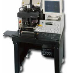
The Mask Aligner (tool #15) is a Karl Suss Model MA-6. This Aligner is a contact printer capable of 1 micron resolution or better, using standard lithographic techniques. Substrates up to 6" in diameter can be used with tooling available for small sample pieces. The mask aligner places an image onto the substrate with precision alignment capability and then exposes the photosensitive resist through a mask with ultra-violet light. The substrate is subsequently developed, exposing the specific pattern for further etching or plating processes. Alignment is achieved manually to an accuracy of <0.25 microns. Alignment modes include vacuum contact for highest resolution and soft contact for minimum substrate damage.
-
Tool #15A Quintel Mask Aligner
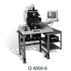
The Mask Aligner (tool #15A) is a Quintel Model Q4000-6. This supplemental Aligner is also a contact printer capable of 1 micron resolution like the Suss MA6. Configured with Deep UV exposure, and UV/IR backside alignment capability, this system will provide a redundant tool for a high utilization area of the clean room. Substrates up to 6" in diameter can be used with tooling available for small sample pieces. Alignment modes include vacuum contact for highest resolution and soft contact for minimum substrate damage.
-
Tool #21 Nikon L150 Optical Microscope
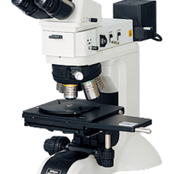
A manual, nosepiece type microscope which meets the various needs of observation, inspection, research and analysis across a wide range of industrial fields. Higher NA and a longer working distance than ever before means superior optical performance and efficient digital imaging.
Maximum sample size: 150 x 150 mmThe Microscope has been fitted with an Omax 5.0mp digital camera and Toup View software for image measurement.
-
Tool #21A Optical Scope w/ Film Thickness Measurement
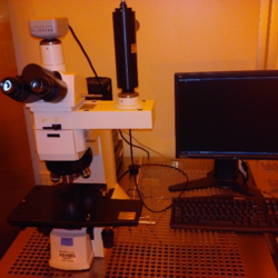
A manual, nosepiece type microscope which meets the various needs of observation, inspection, research and analysis across a wide range of research fields. Higher NA and a longer working distance than ever before means superior optical performance and efficient digital imaging. Maximum sample size: 150 x 150 mm
The Microscope has also been fitted with a Filmetrics F40 transparent thin film thickness measurement system. The very fast metrology system compares the reflectance spectrum of a measured thin film to a theoretically computed model of a material in order to obtain thickness information of the film, including oxide, nitride, photoresist, polysilicon and other transparent films.
-
Tool #58 Focused Ion Beam (FIB)
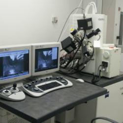
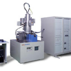
The Focused Ion Beam Milling system (FIB, tool #58) is a Leo XB1540. This workstation combines the imaging capabilities of the GEMINI field emission column with a high performance focused ion beam. Features include a comprehensive gas injection system for ion beam deposition of metals or insulators and for enhanced etching, infra-red CCD cameras and 5-dimensional stage for live specimen handling and navigation monitoring. This tool provides analytical capabilities, TEM sample preparation, cross section investigation, three- dimensional structural examination and fabrication, failure analysis and MEMS fabrication capability.
There is currently no Procedure Manual available for download for this tool.
-
Tool #58A Oxford Instruments INCA EDS
Oxford Instruments have designed hardware for the INCA platform which combines excellence in both detector and pulse processor performance. Hardware designed specifically to give the high quality, stable output required for accurate, automatic peak identification, and standardless, quantitative analysis over a range of useful count rates. Our EDS detectors, the INCAx-stream digital pulse processor and the INCAEnergy EDS software combine in total harmony to make INCA a complete system that works accurately and productively.
There is currently no Procedure Manual available for download for this tool.
-
Tool #58B Oxford Electron Backscatter Detector (EBSD)
Further enhancing the Cross-beam workstation is an Electron Backscatter Defraction (EBSD) system from Oxford Instruments. The tool provides enhanced micro-structure, grain and crystallographic information from samples including crystal mimic, pattern optimization, crystal orientation in grains, and mapping and measurement.
There is currently no Procedure Manual available for download for this tool.
-
Tool #58C Scanning Transmission Electron Microscopy
The Zeiss STEM extends our existing SEM capabilities to the sub-nanometer range and provides images similar to TEM with less chance of damage to the sample and greater ease of operation. This single facility can now prepare TEM samples and the multi-mode STEM detector is mounted on a completely retractable assembly fitted with a high precision adjustment so that optimum alignment can be obtained and can be used in combination with all other Gemini detectors within the system.
The multi-mode STEM detection system enables simultaneous separate BF, DF and orientated DF (ODF) signals, without any need for realignment during imaging. Non-conducting specimens, non stained organic material, or ceramics can be imaged in VP mode without any charging effects.
There is currently no Procedure Manual available for download for this tool.
-
Tool A2 C/V Stress (plotter)
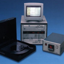
Accuracy and control are the key words for MDC production C-V measurements. The user can select from three different data gathering modes: Swept, Retrace or Pulsed. Each mode examines the MOS device under different conditions. The Swept Mode finds the substrate doping, flatband voltage, threshold voltage, and mobile ion concentration. An important feature of the Swept Mode is the Light Flash and Stabilization. This assures that the MOS device has reached equilibrium inversion capacitance before the sweep begins. Since the C-V sweep begins with the MOS device in inversion, errors due to sweeping rate and inversion capacitance determination while sweeping are eliminated. The result is a "textbook" C-V plot with no anomalous glitches. The Retrace mode shows hysteresis
-
Tool A3 Thin film stress gauge
Dektak Software pkg. with Dektak 8
-
Tool #23 Surface Profilometer
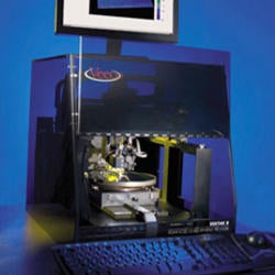
The Surface Profilometer (tool #23) and Thin Film Stress Gauge (tool #A3) are combined in one tool - the Veeco systems Dektak 8. The system is a Bench-Top Surface Profiler that measures the step heights of any surface, with a programmable stylus, which applies a force down to 1 milligram and a Z-height capability up to 1 millimeter. It has a low-inertia sensor to deliver extremely accurate step heights, surface roughness, and waviness measurements on samples up to 8 inches in diameter. Advanced 3D data analysis software for surface characterization of MEMS, semiconductors and other thin/thick films. The system provides 7.5 angstrom, 1 sigma step height repeatability. Stress measurements are achieved by measuring the curvature profile of a substrate before and after a given process step. The software allows the calculation of the added stress based on the known material properties and variations in curve profile.
-
Tool #76 3D Surface Profilometer
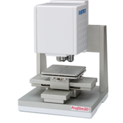
The Profilm3D has sub-nanometer vertical resolution, which surpasses optical profilometers that cost 3x as much. It does so by using the same state-of-the-art measurement technologies as the most sensitive optical profilers available: vertical-scanning interferometry (VSI) and phase-shifting interferometry (PSI). The Profilm3D includes intuitive software for measuring surface roughness, topography, and step heights. In seconds, you can measure all common roughness parameters, on both flat and curved surfaces. The system requires reflective surfaces for accurate measurements but can be used in conjunction with the Filmetrics F40 film thickness system to measure transparent films as well.
-
Tool #24B Ellipsometer
The Ellipsometer system (tool #24B) is a UVISEL Spectroscopic Phase Modulated Ellipsometer (SPME) that incorporates a photo-elastic device to modulate the polarization without any mechanical movement. The UVISEL FUV extends the range of measurements down to 190 nm. The FUV200 integrates two different detectors (solar blind and UV/vis PMT detectors) to provide an extremely low level of stray light. Combined with high throughput optics, this ellipsometer provides very high sensitivity and precision without compromise. The FUV range is often required for lithography applications, characterization of metals, high k dielectrics and organic materials as well as increased sensitivity to ultra-thin films.
-
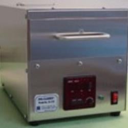
Tool #73 Hi Q Engineering UltraViolet Ozone Cleaner
The UVO method is a photo-sensitized oxidation process in which the contaminant molecules of photo resists, resins, human skin oils, cleaning solvent residues, silicone oils, and flux are excited and/or dissociated by the absorption of short-wavelength UV radiation. Atomic oxygen is simultaneously generated when molecular oxygen is dissociated by 184.9 nm and ozone by 253.7 nm uv. The 253.7 nm UV radiation is absorbed by most hydrocarbons and also by ozone. The products of this excitation of contaminant molecules react with atomic oxygen to form simpler, volatile molecules which desorbs from the surface. Therefore, when both UV wavelengths are present atomic oxygen is continuously generated, and ozone is continually formed and destroyed. By placing properly pre-cleaned samples within five millimeters of ozone producing UV source, such as the low pressure mercury vapor grid lamp in the UVO-Cleaner ®, near atomically clean surfaces can be achieved in less than one minute. The process does not damage sensitive device structures of MOS gate oxide.
-
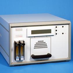
Tool #1 EMS 1050X Plasma Asher
The Tabletop Plasma Etcher (tool #1) is an EMS model 1050X. This convenient single wafer system is a small reactor that consists of a solid state RF generator and associated tuning circuits, a vacuum system with solenoid valves, a constant feed gas supply system and a reaction chamber which includes two semicircular electrodes and a two piece Pyrex chamber. The unit capable of controlling two process gases and is currently configured with pure Oxygen only, connected Gas control #1.
The plasma process is accomplished through the use of low pressure, RF induced gaseous discharge. The specimen is loaded into the reaction chamber, the chamber is evacuated, a carrier gas (Oxygen) is introduced into the chamber raising the pressure to 5x10⁻¹ to 1x10 0 mbar, depending on the application. RF power is applied around the chamber at 13.56MHz. This excites the carrier gas molecules and dissociates it into chemically active atoms and molecules. This ionization process occurs at relatively low temperatures without employing toxic chemicals and is excellent at removing (ashing) organic materials.
-
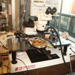
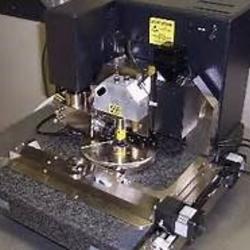
Tool #25B IV Probe station
The I/V Probe Station (tool #25B) Consists of a Signatone S1160 probe station and Agilent E5270A Analyzer. This is a desktop low current low-noise system for DC and AC characterization, and failure analysis on semiconductor wafers and devices. The unit is equipped with X-Y and Z probe micro-positioning, operator microscope and will accept both magnetic base and vacuum base micro-positioners. The Agilent precision DC parametric analyzer with source-monitor-unit (SMU) plug-ins provide current ranges from fempto-Ampère (1E-15) to several Ampères, and potentials from micro-Volt to the hundreds of Volts. This allows the full characterization of devices under test in all four I-V quadrants (forward and reverse currents and voltages are measured with the same SMU unit).
There is currently no Procedure Manual available for download for this tool.
-
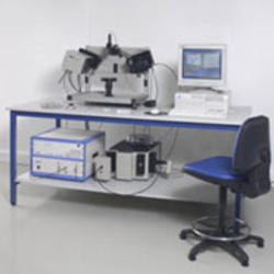
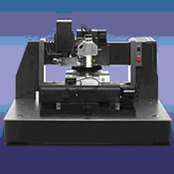
Tool #70 Atomic Force Microscope
The Dimension 5000 scanning probe microscope provides users with the ultimate automated tool for large-sample metrology and imaging. This SPM is capable of measuring up to one hundred areas on samples up to 350mm in diameter. A comprehensive range of AFM and STM techniques enables the Dimension 5000 to detect faults and measure roughness and other features in three dimensions without any sample destruction, pretreatment, or modification. The Dimension 5000 system features an XYZ scanning head that offers up to six times lower Z sensor noise and four times faster scanning than any other closed-loop system available.
-
Tool #70A Atomic Force Microscope
General Information and Usage
The Dimension 3100 Nanoman AFM from Veeco provides a variety of high resolution surface imaging techniques and the ability to manipulate or create nanoscale structures directly. Techniques available for imaging include contact mode AFM, tapping mode AFM, Scanning Tunnelling AFM, Conductive AFM, and Scanning Capacitance Microscopy. With the Nanoman option, the X and Y deflecting piezo-elements are independently controlled, allowing for precise and direct placement of the tip anywhere within the field. Direct manipulation of particles on the surface is then possible by dragging the tip in the desired direction. This feedback control, coupled with direct control of conductive tip and substrate voltages, allows for direct-write oxidation on a variety of surfaces to create or modify nanostructures through local anodization.
Detailed Specifications
- Conductive AFM modules for nA-microAmp current measurements
- Tunneling AFM modulefor pA-nA current measurements
- Scanning Capacitance Microscopy
- Resolution: Sub-nm height-measurement capability; X-Y resolution tip dependent
- Registration tolerance to a known mark: Field size dependent
- Minimum substrate size: small pieces
- Largest substrate size: 100 mm wafer
- Procedure Manual
Lithography
-
Tool #16 Resist Coat Spin Station
The Photo-Resist Spin Coat station (tool #16) is a custom designed tool that applies a layer of photosensitive material (photoresist) to the substrates. The substrates are placed on a vacuum chuck and droplets of photoresist are placed in the center. The chuck is then spun at high speed with centrifugal force and surface tension determining the thickness of the resulting layer. The substrates are then placed on a hotplate to cure the resist prior to the mask alignment step. Both Positive and Negative chemistries are available.
Data Sheets/Reference Material
-
Tool #13 8' Wet Bench (acid)
The Acid Wet Bench (tool #13) is a custom-built state of the art workstation for providing an area to safely process wafers up to 6'' in diameter through wet acid processes, dump and cascade rinse baths. The system is designed to be flexible enough to allow for batch or small individual sample processing so as to minimize the use of chemicals. The station is also equipped with process timers and an aspirator to remove waste acids directly to an external acid waste neutralization system.
There is currently no Procedure Manual available for download for this tool.
-
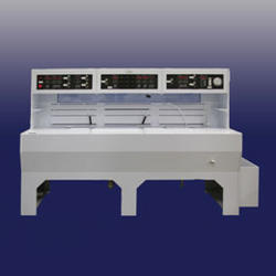
Tool #7A 7' Wet bench (base)7' Wet bench (base)
The Base Wet Bench (tool 7#A) is similar to the Acid Wet Bench in that it is constructed of polypropylene for chemical resistance and durability. This workstation is designed as an area to safely process substrates through base chemicals that include strippers and developers. The same safety and process features apply to both wet benches.
There is currently no Procedure Manual available for download for this tool.
-
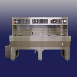
Tool #7B 6' Solvent Bench
The Solvent Bench (tool #7B) is a custom-built state of the art workstation for safely providing an area for solvent cleaning and stripping, non-acid pre-cleaning and wet developing of negative photoresist. This ventilated station is constructed of stainless steel and is also equipped with solvent heating capabilities, process timers, automatic drains to individual reservoirs, and a fire suppressant system for maximum safety.
There is currently no Procedure Manual available for download for this tool.
-
Chemical Processing Station
The Chemical Processing Spin Station is a standalone spinner configured to deliver wet chemicals to the surface of the substrate in a controlled safe manner. The system will be configured for sulfuric acid/hydrogen peroxide mixing to clean the surface of the wafer. The operator simply places the dry wafer onto the spin chuck, selects the preferred recipe, and the system will dispense the chemical, rinse and dry the part. The operator never comes into contact with the chemicals.
There is currently no Procedure Manual available for download for this tool.
-
Tool #9 E-beam Lithography System
The SEM/E-beam Lithography system (tool #9) is a Leo SUPRA 55 with electron-beam pattern generation capability. The combination of ultra-high resolution imaging, patterning and analytical capabilities gives the system exceptional versatility. This tool provides 12x to 900,000x magnification and is capable of producing patterns on components or photo-masks with resolutions from 4nm at 1kv to 1nm at 15kv.
-
Tool #9A E-beam Direct Write Lithography System
The JBX-5500FS (Tool 9A) is a high resolution direct write tool that is PC-controlled and simple to use. A spot beam, vector scan system, the JBX-5500FS writes patterns at a minimum line width of 10nm at 50kV and up to 3 inches in diameter on stitched patterns.
The JBX-5500FS can achieve writing accuracies in two separate modes:
- High Resolution Mode: Overlay accuracy of < 40nm (3 sigma) can be achieved at 50kV.
- High Speed Mode: High speed mode allows 1mm fields at 50kV or 2mm at 25kV.
- The JBX-5500FS can accept parts/pieces and wafers up to 100mm substrates via a single wafer manual loader.
There is currently no Procedure Manual available for download for this tool.
-
Tool #9B Mask Design Station
The Mask design station is a PC system with L-edit software available for mask design. Use your own autocad design and convert to mask generating format.
There is currently no Procedure Manual available for download for this tool.
Miscellaneous
-
Tool #74 WestBond 7700E Wire Ball Bonder
UNLIMITED DEEP REACH access to remote bond targets on large packages with WEST·BOND’S new throat-less chassis and micromanipulator designs. All machine components, circuitry and enclosures are arrayed above the horizontal bond plane, eliminating any restrictions to package size or shape. Manual “E” Series models are available for all microwave, semiconductor, R.F., and hybrid production, and are ideal for repair station or laboratory use.
Supplied with .001” gold wire or aluminum on request.
-
Tool #75 K&S 4523A Digital Wedge Bonder
The Model 4526 Auto-Step-back Wedge Bonder is used with gold wire. It is especially appropriate for high quality applications requiring tight control of wire length and loop formation. The 4526 offers control of individual bond parameters and programmable loop formation along with the capability of using a wide variety of wires. The bonding head, with the deep access option and tail adjust system, makes it ideal for deep cavity microwave applications where tight control over the tail length is required.
