
About
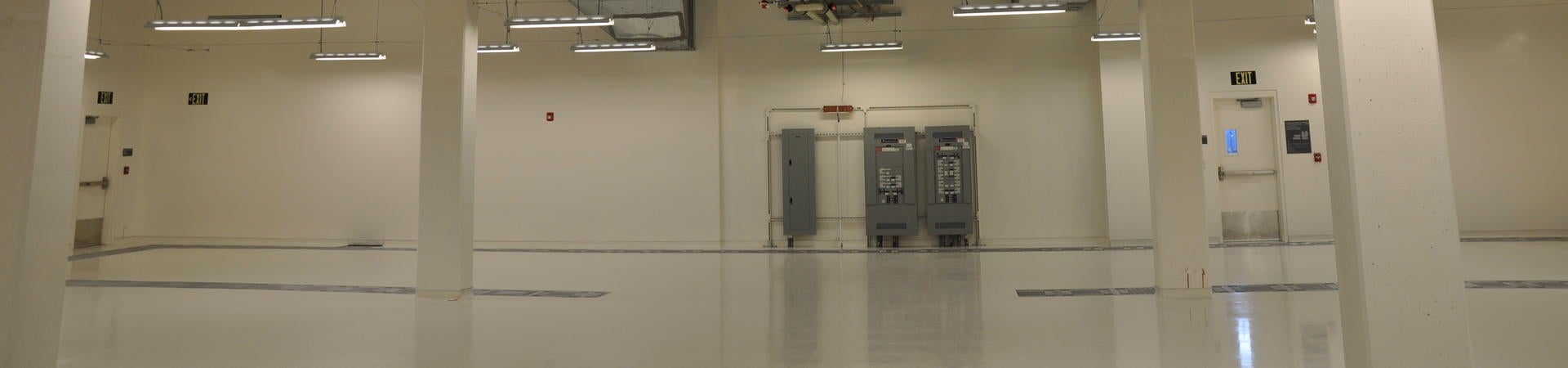
The UCR Nanofabrication Facility currently operates two Nanofabrication Cleanroom facilities on the UCR campus. The first is located in the lower level of the B wing of Bourns Hall. It is a state-of-the-art Nanofabrication Research facility available 24/7 to qualified users. The facility is approximately 2,000 square feet and includes significant safety and operational monitoring capabilities. Our second Cleanroom is located in the new Materials Science and Engineering building on the lower level. The class 100/1000 space occupies approximately 8,000 square feet and currently two small bays are functional with the initial few tools installed.
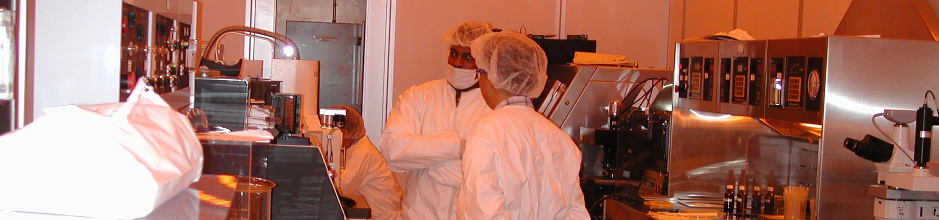
At present, the Bourns Hall Cleanroom is fully operational and certified at Class 100 in the Photolithography bay, Class 1000 in the Thin Film/Etch bay and the environment is being controlled and monitored. There is a trained staff of 3 full-time engineers available to users at no charge from 9-5p.m. weekdays. There are currently over 100 trained users conducting research in various fields of engineering and sciences from Physics, Chemistry, Environmental, Chemical, Mechanical and Electrical Engineering. The facility is also available to industrial users for research projects in other fields.
The following tools are presently available for training and/or use:
- E-beam Lithography Systems
- Focused Ion Beam System
- EBSD
- EDAX
- STEM
- Plasma Enhanced CVD System
- Rapid Thermal Anealer
- STS Reactive Ion etcher
- Atomic Layer Deposition
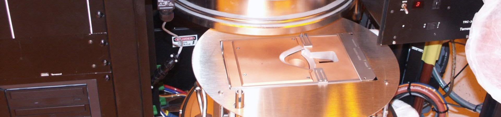
- E-beam Evaporation
- Sputtering
- Thermal Evaporation
- Dektak Profilometer
- C/V Plotter
- I/V Probe Station
- Plasma Asher
- Ellipsometer
- Filmetrics Thickness Measurement
- Atomic Force Microscope
- Quintel Mask Aligner
- Suss MA-6 Mask Aligner
- Photoresist Spin Coat Station
- Wire Bonding
- Base Development Wet Bench
- Solvent Wet Bench
- U/V Ozone Cleaning
- Scanning Electron Microscope (SEM)